Brian's TI Voyage™ 200 Hardware
Page
The idea for this page is, I admit, a rip-off of this page: The
Hardware of a TI-89 which has long since been deleted (but I've linked to it
on WayBackMachine so that, hopefully, you
can still see it).
Since I haven't actually stolen any of the
information from that page you will still need to go there, or elsewhere, for most of the
interesting detail about TI-89, TI-92+ and Voyage 200 hardware.
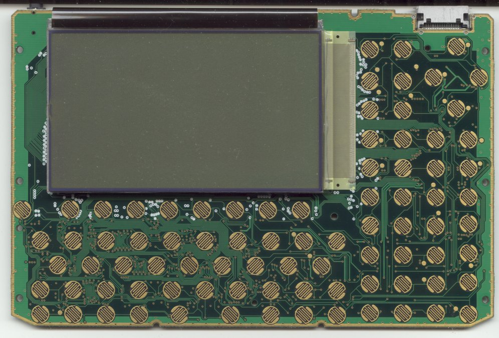
However I have something which isn't on that page -- photos of the inside of
my Voyage 200...
Voyage™ 200 Circuit Board Back View:

View/Download JPEG image: small(61KB) medium(218KB)
large(699KB) extra-large(2.3MB)
Notes (mine, not guaranteed to be 100% correct):
- U1 & U2 are Toshiba T6B08 - row drivers for a dot matrix LCD
- U3, U4 & U5 are Toshiba T6B07 - column drivers for a dot matrix LCD
- U6 & U7 are 128K*8 (128K byte) CMOS RAM chips (static RAM)
- U8 is a Sharp LH28F320BFHE-PBTLZ2 - a 4M byte Flash memory
- U9 is a Motorola MC68SEC000PB16 processor. (A low power CMOS version of the 68000)
- U10 is probably a custom chip of some kind
- U11 is marked HC14A - presumably six inverting buffers
- U15 is LP324M - four low power operational amplifiers
- U16 is 74HCT244 - eight tri-state buffers
- U17 is 74HC00 - four nand gates
- J3 is the Graphlink socket
- X1 is a 32.768kHz crystal for the real time clock
- BATT1 - these gold contacts are where the 6V from the four AAA cells connects to the board
- The round gold pad inside the white rectangle and the smaller square gold pad just above D4 are where the 3V from the lithium memory backup button cell connects to the board
Voyage™
200 Circuit Board Front View:

View/Download JPEG image: small(48KB) medium(169KB)
large(560KB) extra-large(1.8MB)
Click here to go back to my Home Page

Click this advert, and sign up and you and Brian should both get a gift card or a free month.
Brian uses this plan:


